 |
| Fig.1 CMOS Inverter Construction |
And PMOS will let low voltage pass while NMOS will let high voltage pass. Therefore, the maximum output voltage (VOH=VDD) occurs when input voltage is low (Vin=0V) PMOS is on and pulls Vout to VDD while NMOS is off. Moreover, the minimum output voltage (VOL=0V) occurs when input is high (Vin=VDD) NMOS is on and pulls Vout to ground while PMOS is off. Thus,there is a transition region between VOH and VOL and there are three situations:
1. If input voltage (Vin) is low:
- When 0≤ Vin < VTN (threshold voltage of NMOS)
- Mn (N-channel) in cut off and off
- Mp (P-channel) in triod and Vout is pulled to VDD
- When
`VH}(LLG1DM.jpg) VTN≤Vin<Vo一|VTP| (threshold voltage of PMOS)
VTN≤Vin<Vo一|VTP| (threshold voltage of PMOS)
- Mn in saturation with strong current
- Mp in triode and VSGp (voltage on Mp) and current reducing
- Vout decreases via current through Mn
2. If Vin = Vout (mid point) ≈ 0.5 VDD
- Mn and Mp both in saturation
- Maximum current at Vin = Vout
3. If Vin is high
- When Vout + VTN ≤ Vin <VDD - |VTP|
- Mn in triode, Mp in saturation
- When Vin> VDD -|VTP|
- Mn in triode, Mp in cut off
And the CMOS inverter voltage transfer characteristic curve according to the situation above is shown in below:
 |
Fig.2 0P0JQ8LTLNM`TF)M9ZW.jpg) CMOS Inverter Voltage Transfer Characteristic Curve CMOS Inverter Voltage Transfer Characteristic Curve |
In order to simulate the curve above through MATLAB, the following equations will be applied:
1. The current equation of PMOS is :
- Cut-off region: i=0
- Saturation region:
FTK.jpg)
FTK.jpg)
FTK.jpg)
 |
| (2) |
- Linear region:
 |
| (3) |
2. The current equation of NMOS is:
- Cut-off region: i=0
- Saturation region:
 |
| (5) |
- Linear region:
 |
| (6) |
As for a no-load CMOS inverter: ipmos = inmos
(7)
And βp is the transconductance coefficient of PMOS which has the equation:
μp is the electron mobility in p-type semiconductor and Cox is the unit capacitance of gate oxide layer and (W/L)p is the aspect ratio of the PMOS Gate.
βN is the transconductance coefficient of NMOS which has the equation:
μN is the electron mobility in n-type semiconductor and Cox is the unit capacitance of gate oxide layer and (W/L)n is the aspect ratio of the NMOS Gate.
Therefore,
(1) When 0≤ Vin < VTN,
Simultaneous equations (3) (4) (7) can get the following equation:
Vo = VDD
(2) When %60VH%7D(LLG1DM.jpg) VTN≤Vin<Vo一|VTP|,
VTN≤Vin<Vo一|VTP|,
%60VH%7D(LLG1DM.jpg) VTN≤Vin<Vo一|VTP|,
VTN≤Vin<Vo一|VTP|,
Simultaneous equations (3) (5) (7) can get the follwing equation:
(3)When Vo-|VTP| < Vin<Vo+VTN,
Simultaneous equations (2) (5) (7) can get the following equation:
consider the linearity current change of PMOS and CMOS and no-load CMOS inverter mode, can get the following equation:
(4)When Vout + VTN ≤ Vin <VDD - |VTP|,
Simultaneous equations (2) (6) (7) can get the following equation:
(5)When Vin> VDD -|VTP|
Simultaneous equations (1) (6) (7) can get the following equation:
Vo = 0V
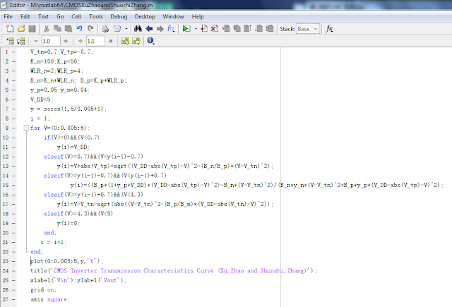
Thus, the MATLAB code desiged by the experimenter to show the CMOS inverter voltage transfer characteristic curve is shown in figure below:
 |
| Fig.3 MATLAB Code for CMOS inverter voltage transfer characteristic curve |
After running he program, experimenters can get the waveform as shown in the figure below:
| Fig.4 CMOS inverter voltage transfer characteristic curve |
According to the figure above Fig.4 is similar to Fig.2,which verify the simulation waveform simulated by the experimenter is successful.


Hey, nice blog. Could you please let me know where you got the equations for the output voltage you used in the model.
ReplyDeleteThank you.
what is y_p and y_n ?
Delete